Microelectronics Fabrication
Wafer-level photolithography, integrated circuit patterning, and multi-layer device fabrication.
Compact LED-based exposure and masking system for high-resolution photolithography with 500nm capability and universal photoresist compatibility.
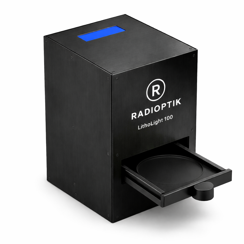
The LithoLight exposure and masking system is a compact, high-performance solution for photolithography applications. Available in 4" or 6" versions, it features an LED-based optical head providing collimated and homogeneous illumination.
LithoLight is suited for prototype development, photonics work, microfabrication, and small-batch manufacturing where consistent pattern fidelity matters.
Wafer-level photolithography, integrated circuit patterning, and multi-layer device fabrication.
High-precision patterning for MEMS device fabrication and optical sensor manufacturing.
Optical element patterning, photonic device manufacturing, and waveguide fabrication.
Flexible support for prototyping, nanotechnology research, and small-batch development workflows.
LithoLight works seamlessly with popular photoresist families, giving you flexibility across research and manufacturing workflows.
Contact our team to discuss your photolithography requirements and discover how LithoLight can support your manufacturing process.
Contact Our Team